GPU Memory Hierarchy
Understanding cache levels, access patterns, and bandwidth optimization for CUDA programming
1. GPU Memory Hierarchy
Modern NVIDIA GPUs have a multi-level memory hierarchy. Each level trades off capacity for speed. Understanding this hierarchy is critical for writing high-performance CUDA code.
~20 TB/s effective
256 KB per SM
~1 cycle latency"] L1["L1 Cache + Shared Memory
~12-19 TB/s
128-256 KB per SM
~30 cycles latency"] L2["L2 Cache
~6-8 TB/s
48-96 MB total
~200 cycles latency"] end HBM["HBM (VRAM)
~3.35 TB/s (H100)
80-192 GB total
~400+ cycles latency"] REG --> L1 L1 --> L2 L2 --> HBM style REG fill:#76B900,stroke:#76B900,color:#000 style L1 fill:#22c55e,stroke:#22c55e,color:#000 style L2 fill:#3b82f6,stroke:#3b82f6,color:#fff style HBM fill:#6366f1,stroke:#6366f1,color:#fff
Bandwidth Comparison (H100 SXM)
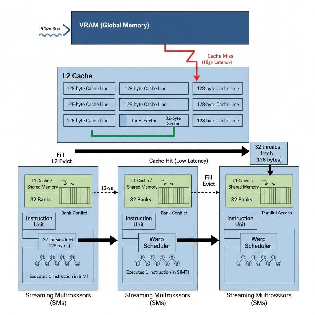
Data Path: Global Memory → L2 → Streaming Multiprocessors
Data flows from VRAM (global memory) through the L2 cache to the SMs. A cache miss causes a high-latency fetch from VRAM into a 128-byte L2 cache line; a cache hit keeps access low latency. A warp (32 threads) typically fetches 128 bytes at a time. Inside each SM, L1/shared memory is organized in 32 banks—bank conflict serializes accesses when threads hit the same bank; parallel access occurs when threads use different banks.
2. Cache Line Architecture
L2 Cache Organization
| Total Size | 50-96 MB |
| Cache Line Size | 128 bytes |
| Floats per Line | 32 floats (4B each) |
| Associativity | 16-32 way set-associative |
| Sectors per Line | 4 × 32B sectors |
Cache Line Layout
32B"] S2["Sector 1
32B"] S3["Sector 2
32B"] S4["Sector 3
32B"] end style S1 fill:#76B900,stroke:#76B900,color:#000 style S2 fill:#22c55e,stroke:#22c55e,color:#000 style S3 fill:#3b82f6,stroke:#3b82f6,color:#fff style S4 fill:#6366f1,stroke:#6366f1,color:#fff
Memory Layout: Cache Lines with Floats
3. Access Patterns & Cache Efficiency
Sequential Access (stride=1) - Best Case
Every element in the cache line is used. Maximum cache efficiency!
Strided Access (stride=32) - 1 Float per Line
Only 1 float used per cache line. Fetching 128 bytes to use 4 bytes!
Large Stride (stride=1024) - Pure HBM
Stride of 1024 floats = 4KB between accesses. Cache lines are evicted before reuse. This measures raw HBM bandwidth.
(Cache Line 0)"] --> B["Skip 31 lines"] B --> C["Read f1024
(Cache Line 32)"] C --> D["Skip 31 lines"] D --> E["Read f2048
(Cache Line 64)"] E --> F["..."] G["Cache Line 0 evicted
before f32 is ever read!"] style A fill:#ef4444,stroke:#ef4444,color:#fff style C fill:#ef4444,stroke:#ef4444,color:#fff style E fill:#ef4444,stroke:#ef4444,color:#fff style G fill:#1e293b,stroke:#64748b,color:#94a3b8
Why L2 Can't Help
- • L2 Size: 96 MB, but tensor is 256 MB
- • Access Gap: 4KB between accesses = 32 cache lines skipped
- • Result: By the time loop returns to reuse data, it's been evicted
- • Every read: Goes to HBM (400+ cycle latency)
4. Stride vs Bandwidth Summary
| Stride | Bytes Skipped | Cache Efficiency | Measured BW | What's Happening |
|---|---|---|---|---|
| 1 | 4 bytes | ~100% | ~2500 GB/s | L2 cache serves most requests |
| 32 | 128 bytes | 3.125% | ~1800 GB/s | 1 float per cache line used |
| 128 | 512 bytes | ~1% | ~1200 GB/s | L2 thrashing begins |
| 512 | 2 KB | ~0% | ~900 GB/s | Mostly HBM |
| 1024+ | 4 KB+ | 0% | ~800 GB/s | Pure HBM (no cache benefit) |
5. Practical Implications
✓ When Cache Helps
- • Sequential/coalesced access - stride=1
- • Dense matrix operations - GEMM, convolutions
- • Working set fits in L2 - <96 MB on H100
- • Data reuse - same data accessed multiple times
✗ When Cache Can't Help
- • Sparse matrix operations - random access
- • Embedding lookups - scattered indices
- • Large stride patterns - stride >128
- • Working set exceeds L2 - streaming data
Optimization Strategies
Ensure threads access adjacent memory locations for maximum cache line utilization.
Process data in chunks that fit in L2/shared memory to maximize reuse.
Use async copies (TMA, cp.async) to hide memory latency.